- 您现在的位置:买卖IC网 > Sheet目录329 > IDT70V5388S166BGI (IDT, Integrated Device Technology Inc)IC SRAM 1.125MBIT 166MHZ 272BGA
IDT70V5388/78
3.3V 64/32K x 18 Synchronous FourPort? Static RAM
Industrial and Commercial Temperature Ranges
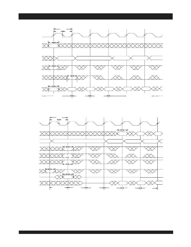
Timing Waveform of Write with Address Counter Advance (1)
t CYC2
CLK
t CH2
t CL2
t SA
t HA
ADDRESS
An
INTERNAL (3)
ADDRESS
An (7)
An + 1
An + 2
An + 3
An + 4
t SCLD t HCLD
CNTLD
t SCINC t HCINC
CNTINC
t SD t HD
DATA IN
Dn
Dn + 1
Dn + 1
Dn + 2
Dn + 3
Dn + 4
WRITE
EXTERNAL
ADDRESS
WRITE WRITE
WITH COUNTER COUNTER HOLD
WRITE WITH COUNTER
5649 drw 14
Timing Waveform of Counter Reset (2)
t CYC2
t CH2
t CL2
CLK
t SA t HA
(4)
ADDRESS
An
An + 1
An + 2
INTERNAL (3)
ADDRESS
Ax
A 0
A 1
An
An + 1
t SW t HW
R/ W
CNTLD
t SCLD t HCLD
CNTINC
t SCRST t HCRST
t SCINC t HCINC
CNTRST
DATA IN
(5)
t SD
t HD
D 0
DATA OUT
Q 0
Q 1
Qn
EXECUTE
CNTRST
(6)
WRITE
A 0
READ
A 0
READ
A 1
READ
ADDRESS n
READ
ADDRESS n+1
5649 drw 15
NOTES:
1. CE 0, LB , UB , and R/ W = V IL ; CE 1 and CNTRST , MRST , MKLD , MKRD , and CNTRD = v IH.
2. CE 0 , LB , UB = V IL ; CE 1 = V IH .
3. The "Internal Address" is equal to the "External Address" when CNTLD = V IL and equals the counter value when CNTLD = V IH .
4. Addresses do not have to be accessed sequentially since CNTLD = V IL constantly loads the address on the rising edge of the CLK; numbers are for reference
use only.
5. Output state (High, Low, or High-impedance) is determined by the previous cycle control signals.
6. No dead cycle exists during CNTRST operation. A READ or WRITE cycle may be coincidental with the counter CNTRST cycle: Address 0000h will be
accessed. Extra cycles are shown here simply for clarification. For more information on CNTRST function refer to Truth Table II.
7. CNTINC = V IL advances Internal Address from ‘An’ to ‘An +1’. The transition shown indicates the time required for the counter to advance. The ‘An +1’Address
is written to during this cycle.
17
6.42
发布紧急采购,3分钟左右您将得到回复。
相关PDF资料
IDT70V631S10PRFG
IC SRAM 4MBIT 10NS 128TQFP
IDT70V639S12PRFI
IC SRAM 2.25MBIT 12NS 128TQFP
IDT70V659S12DRI
IC SRAM 4MBIT 12NS 208QFP
IDT70V7319S166BCI
IC SRAM 4MBIT 166MHZ 256BGA
IDT70V7339S166BCI
IC SRAM 9MBIT 166MHZ 256BGA
IDT70V7519S166DRI
IC SRAM 9MBIT 166MHZ 208QFP
IDT70V7599S133DRI
IC SRAM 4MBIT 133MHZ 208QFP
IDT70V9089L6PF
IC SRAM 512KBIT 6NS 100TQFP
相关代理商/技术参数
IDT70V5388S166BGI8
功能描述:IC SRAM 1.125MBIT 166MHZ 272BGA RoHS:否 类别:集成电路 (IC) >> 存储器 系列:- 标准包装:3,000 系列:- 格式 - 存储器:EEPROMs - 串行 存储器类型:EEPROM 存储容量:8K (1K x 8) 速度:400kHz 接口:I²C,2 线串口 电源电压:1.7 V ~ 5.5 V 工作温度:-40°C ~ 85°C 封装/外壳:8-SOIC(0.154",3.90mm 宽) 供应商设备封装:8-SOIC 包装:带卷 (TR)
IDT70V5388S200BC
功能描述:IC SRAM 1.125MBIT 200MHZ 256BGA RoHS:否 类别:集成电路 (IC) >> 存储器 系列:- 标准包装:3,000 系列:- 格式 - 存储器:EEPROMs - 串行 存储器类型:EEPROM 存储容量:8K (1K x 8) 速度:400kHz 接口:I²C,2 线串口 电源电压:1.7 V ~ 5.5 V 工作温度:-40°C ~ 85°C 封装/外壳:8-SOIC(0.154",3.90mm 宽) 供应商设备封装:8-SOIC 包装:带卷 (TR)
IDT70V5388S200BC8
功能描述:IC SRAM 1.125MBIT 200MHZ 256BGA RoHS:否 类别:集成电路 (IC) >> 存储器 系列:- 标准包装:3,000 系列:- 格式 - 存储器:EEPROMs - 串行 存储器类型:EEPROM 存储容量:8K (1K x 8) 速度:400kHz 接口:I²C,2 线串口 电源电压:1.7 V ~ 5.5 V 工作温度:-40°C ~ 85°C 封装/外壳:8-SOIC(0.154",3.90mm 宽) 供应商设备封装:8-SOIC 包装:带卷 (TR)
IDT70V5388S200BCG
功能描述:IC SRAM 1.125MBIT 200MHZ 256BGA RoHS:是 类别:集成电路 (IC) >> 存储器 系列:- 标准包装:3,000 系列:- 格式 - 存储器:EEPROMs - 串行 存储器类型:EEPROM 存储容量:8K (1K x 8) 速度:400kHz 接口:I²C,2 线串口 电源电压:1.7 V ~ 5.5 V 工作温度:-40°C ~ 85°C 封装/外壳:8-SOIC(0.154",3.90mm 宽) 供应商设备封装:8-SOIC 包装:带卷 (TR)
IDT70V5388S200BG
功能描述:IC SRAM 1.125MBIT 200MHZ 272BGA RoHS:否 类别:集成电路 (IC) >> 存储器 系列:- 标准包装:3,000 系列:- 格式 - 存储器:EEPROMs - 串行 存储器类型:EEPROM 存储容量:8K (1K x 8) 速度:400kHz 接口:I²C,2 线串口 电源电压:1.7 V ~ 5.5 V 工作温度:-40°C ~ 85°C 封装/外壳:8-SOIC(0.154",3.90mm 宽) 供应商设备封装:8-SOIC 包装:带卷 (TR)
IDT70V5388S200BG8
功能描述:IC SRAM 1.125MBIT 200MHZ 272BGA RoHS:否 类别:集成电路 (IC) >> 存储器 系列:- 标准包装:3,000 系列:- 格式 - 存储器:EEPROMs - 串行 存储器类型:EEPROM 存储容量:8K (1K x 8) 速度:400kHz 接口:I²C,2 线串口 电源电压:1.7 V ~ 5.5 V 工作温度:-40°C ~ 85°C 封装/外壳:8-SOIC(0.154",3.90mm 宽) 供应商设备封装:8-SOIC 包装:带卷 (TR)
IDT70V631S10BC
功能描述:IC SRAM 4MBIT 10NS 256BGA RoHS:否 类别:集成电路 (IC) >> 存储器 系列:- 标准包装:2,500 系列:- 格式 - 存储器:EEPROMs - 串行 存储器类型:EEPROM 存储容量:1K (128 x 8) 速度:100kHz 接口:UNI/O?(单线) 电源电压:1.8 V ~ 5.5 V 工作温度:-40°C ~ 85°C 封装/外壳:8-TSSOP,8-MSOP(0.118",3.00mm 宽) 供应商设备封装:8-MSOP 包装:带卷 (TR)
IDT70V631S10BC8
功能描述:IC SRAM 4MBIT 10NS 256BGA RoHS:否 类别:集成电路 (IC) >> 存储器 系列:- 标准包装:3,000 系列:- 格式 - 存储器:EEPROMs - 串行 存储器类型:EEPROM 存储容量:8K (1K x 8) 速度:400kHz 接口:I²C,2 线串口 电源电压:1.7 V ~ 5.5 V 工作温度:-40°C ~ 85°C 封装/外壳:8-SOIC(0.154",3.90mm 宽) 供应商设备封装:8-SOIC 包装:带卷 (TR)
